
1. How can perovskite cells break through the dominance of silicon-based photovoltaics?
As a key part of solar cells, cells determine the efficiency and cost of power generation and are the key to iterative replacement.
As a technology- and capital-intensive industry, the photovoltaic industry is the fastest-growing new energy track in recent years. The entire industry has been rolling up to the sky, and its maturity is no less than that of lithium batteries. The core driving force of its development is cost reduction and efficiency improvement, so the iterative replacement of cell technology has always attracted market attention.
Since the 1950s, photovoltaic materials have always been dominated by silicon. Silicon-based photovoltaic cells have undergone many changes from aluminum back field cells to P-type cells and then to N-type cells, and have gradually approached the theoretical limit of photoelectric conversion efficiency in physics.
As a new technology route, perovskite cells have become a research hotspot in the photovoltaic field with their unique performance and advantages since their discovery. Can perovskite cells become a substitute for silicon?
2. Principle of Photovoltaic Cells
Photovoltaic cells are devices that use the photovoltaic effect of semiconductor materials to convert solar radiation into electrical energy. When sunlight shines on the semiconductor p-n junction, photons are absorbed by the semiconductor material, which stimulates the generation of photogenerated carriers: electron-hole pairs. Under the action of the built-in electric field of the semiconductor, electrons and holes move to the two ends respectively, forming current and voltage, realizing the conversion from solar energy to electrical energy.
3. Photovoltaic Cell Development Stage
At present, the search for clean and sustainable energy has become a global issue. In this context, photovoltaic research has flourished. As a key device, the performance and efficiency improvement of photovoltaic cells are crucial to promoting the widespread application of solar energy.
The development of photovoltaic cells has gone through several stages, from polycrystalline silicon cells to monocrystalline silicon cells, to the second-generation thin-film cells, and then to the third-generation new photovoltaic cells represented by perovskite photovoltaics (PSCs) and organic photovoltaics (OPV). Whether it is the second-generation thin-film battery or the battery of the current new technology route, it is still in the 0-1 stage.
Among these technical routes, perovskite photovoltaic cells have shown great development potential with their high photoelectric conversion efficiency and performance advantages.
4. Perovskite cells
1. What is a perovskite cell?
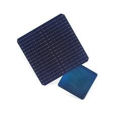
Perovskite cells are solar cells that use organic metal halide semiconductors with perovskite crystal structures as light-absorbing materials. They have the advantages of high photoelectric conversion efficiency, low cost, high weak light efficiency, flexible preparation, thin and translucent, and rich application scenarios.
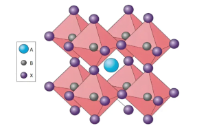
“Perovskite” does not refer to a specific material, but an ABX₃ crystal structure synthesized from common chemical materials, usually composed of metal cations, halogen anions, and organic cations, where the A, B, and X positions can be iteratively replaced. The family of materials that synthesize this crystal structure is collectively referred to as perovskite materials.
Perovskite materials are easy to obtain and cheap, and are artificially synthesized. Their crystal structure is designable and flexible, and they do not require mining and high purification like silicon materials and are restricted by raw materials.
2. Bandgap characteristics
(1) Bandgap type
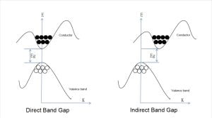
Perovskite cells have a direct band gap, while crystalline silicon cells have an indirect band gap.
Bandgap, also known as energy gap or forbidden band width, refers to the energy difference between the maximum value of the valence band (valence band top) and the minimum value of the conduction band (conduction band bottom), and the minimum energy required for electrons to jump from the valence band to the conduction band. Band gaps are divided into direct band gaps and indirect band gaps. The band gap of solar cells is a key parameter for the absorption and conversion efficiency of light-absorbing materials. It determines the material’s ability to absorb light of different wavelengths.
Direct Band Gap:
When electrons in the valence band transition to the conduction band, it is a vertical transition on the energy band diagram. The momentum remains unchanged during the transition, the light absorption efficiency is high, and a large number of photogenerated carriers are generated, resulting in a higher photoelectric conversion efficiency.
Indirect Band Gap:
This means that the conduction band minimum and the valence band maximum are at different positions in the k-space. When an electron jumps from the valence band to the conduction band, it is necessary not only to change the energy state of the electron but also to change the momentum of the electron, which usually causes part of the energy to be wasted in the form of phonons.
(2) Adjustable band gap:
The composition of perovskite crystals is diverse. By changing the elements and proportions in the ABX3 structure, the band gap width can be adjusted within a certain range. The theoretical range is 1.15-2.8eV, making perovskite surpass crystalline silicon cells in terms of conversion efficiency.
(3) Wide spectral range:
The band gap of a single-junction perovskite solar cell is about 1.5eV, while the band gap of silicon is 1.12eV. The band gap of a perovskite cell is wider than that of a crystalline silicon cell, and the absorption spectrum range is larger, generally covering a wavelength range of about 300nm-800nm, covering visible light and part of near-infrared light.
3. Crystal characteristics
Crystal structure
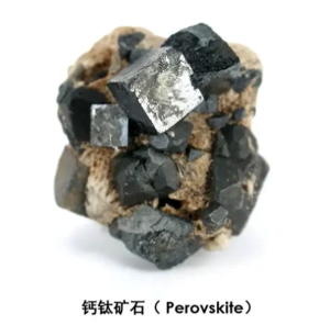
Perovskite materials have a crystal structure similar to calcium titanate (CaTiO₃), which is an artificially synthesized ABX₃ crystal structure. It is a three-dimensional structure composed of monovalent cations A and BX6 octahedrons, where the B position is a divalent metal ion, the X position is a monovalent halogen anion, B is located at the center of the octahedron, surrounded by 6 X ions to form a coordinated cubic octahedron, and A is located at the center of the octahedral gap and surrounded by 12 X anions.
The A position is generally cesium ions, methylamine ions, and formamidine ions. The A position ions mainly compensate for the lattice charge and adjust the perovskite energy band, thereby improving the photovoltaic performance of the device; the B position is generally lead ions and tin ions; the C position is generally chloride ions, bromide ions, iodine ions or multiple halogen ions.
Crystal characteristics
(1) High absorption coefficient
Perovskite materials have a high light absorption coefficient. Their crystal structure restricts the movement of electrons in a specific direction, resulting in enhanced interaction between electrons and photons, which can efficiently absorb photons. The light absorption coefficient is much higher than that of silicon, even up to 10 times higher in some bands, which means that the thickness of the light absorption layer of perovskite cells can be thinner, and it can make full use of sunlight of different wavelengths to improve the collection of photogenerated carriers.
(2) Long carrier diffusion length
Longer carrier diffusion lengths have a positive impact on the performance of solar cell devices. In photovoltaic panels, longer carrier diffusion lengths enable carriers to be transmitted over longer distances, improve carrier collection, reduce charge recombination, and reduce energy loss, thereby improving photoelectric conversion efficiency.
The carrier diffusion length of perovskite cells varies due to factors such as material systems and preparation processes, and is generally between a few hundred nanometers and several microns. For example, studies have shown that the carrier diffusion length of perovskites filled in insulating mesoscopic supports is as high as 5.48μm.
(3) Low exciton binding energy
Exciton binding energy is an important parameter that directly affects the photoelectric conversion efficiency of the battery. Exciton binding energy refers to the binding energy that needs to be overcome when excitons are formed in semiconductors.
The working principle of perovskite solar cells is based on the absorption of light by perovskite materials to generate electron-hole pairs, i.e., excitons. The exciton binding energy of perovskite materials is very small. For example, the exciton binding energy of methylamine lead iodine (MAPbI₃) is 19±3 meV, which can be separated into free carriers at room temperature.
4. Performance
(1) High absorption coefficient:
Perovskite materials have a high absorption coefficient and can efficiently absorb sunlight at a relatively thin thickness, thereby reducing the amount of materials used and reducing costs.
(2) High photoelectric conversion efficiency:
Compared with crystalline silicon cells, perovskite materials can quickly complete the generation of photogenerated carriers, form electron-hole pairs, and break free from the constraints to form free carriers. They also have a longer carrier diffusion length, which can reduce the occurrence of electron-hole pair recombination.
The theoretical photoelectric conversion efficiency of single-junction perovskite cells is about 33%, which is much higher than the 29.4% of crystalline silicon cells. It has currently reached 26%.
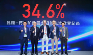
Crystalline silicon perovskite stacked cells, in which perovskite cells are superimposed on the surface of crystalline silicon cells. The top perovskite cell absorbs short wavelengths in sunlight, and the transmitted long wavelengths are absorbed by the narrow-bandgap crystalline silicon cell. This structure reduces energy loss and has a higher theoretical photoelectric conversion efficiency. The theoretical conversion efficiency is about 44%, and the currently certified data is as high as 34.6%.
(3) High weak light efficiency:
Unlike traditional crystalline silicon cells, perovskite cells can still effectively absorb photons and perform photoelectric conversion in weak light environments such as cloudy days, early mornings, evenings, and low-light indoors. This is due to their high light absorption coefficient and wide absorption spectrum range.
This has advantages in some specific scenarios and applications. For example, in indoor environments where the light is not very strong, perovskite cells can also play a role and provide power for small electronic devices, smart homes, etc.
5. Device structure
There are three main types of perovskite cell structures, but many photovoltaic companies mainly choose the trans-planar structure (p-i-n type), which has a relatively simple preparation process, high efficiency and low cost.
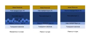
(1) Planar formal structure (n-i-p type): First, an electron transport layer (usually an n-type semiconductor material) is deposited on the transparent electrode, then a perovskite layer is prepared, and then a hole transport layer (usually a p-type semiconductor material) is deposited, and finally a metal electrode. In this structure, the electron transport layer is close to the conductive glass, and the hole transport layer is close to the metal electrode.
(2) Planar inverse structure (p-i-n type): Contrary to the formal planar structure, a hole transport layer is first deposited on the transparent electrode, then a perovskite layer is prepared, and then an electron transport layer is deposited, and finally a metal electrode.
The inverse planar structure has the advantages of simple preparation process, lower film forming temperature, and good compatibility with the stacked battery device structure. It is the mainstream structure used by perovskite battery manufacturers in the industrialization process at this stage.
(3) Mesoporous formal structure (mesoporous n-i-p type): This structure has high stability and photoelectric conversion efficiency.
The mesoporous structure is usually composed of a scaffold layer composed of a mesoporous material (such as TiO2) and a perovskite material filled thereon. Mesoporous materials have high specific surface area and porosity, and their pore size is generally between 2-50nm.
The mesoporous structure can increase the contact area between the perovskite material and light, improve the light absorption rate, provide a good charge transfer channel, help reduce the probability of charge recombination, improve charge collection, and thus improve the photoelectric conversion efficiency (PCE).
The mesoporous structure can protect the perovskite material to a certain extent. Its porosity can play a role in encapsulation and isolation, reduce moisture and oxygen erosion, improve battery stability and life, and suitable mesoporous materials can form a good interface contact with the perovskite, reduce interface defects, and further improve battery stability.
6. Component morphology characteristics
(1) Lightweight and thin: Due to the high absorption coefficient, perovskite cells can be made extremely thin. The thickness of the active layer is usually from a few hundred nanometers to a few microns. Together with other parts such as electrodes and packaging materials, the thickness of the entire component can be within a few millimeters. This is very advantageous in some application scenarios where weight and space are restricted.
(2) Flexibility: It has good flexibility and can be bent and folded, suitable for various flexible electronic devices.
(3) Transparency: It can be chemically modified into colored and translucent films, making the application diversified and meeting different appearance requirements.
7. Preparation and cost
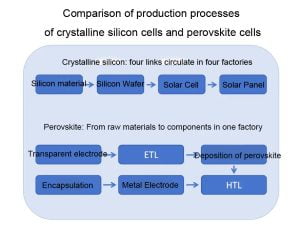
(1) Short preparation process: The preparation process of perovskite cell components is simple and the process is short. The manufacturing from raw materials to components can be completed in a single factory within 45 minutes. However, the silicon materials, silicon wafers, cells, and components of crystalline silicon cells require more than four different factories to produce and process. It takes about three days to complete a component, which is a huge difference in time.
(2) Low production and construction: It is estimated that under the same production capacity, the investment in perovskite cells is about half that of crystalline silicon cells, and 1GW only requires 500 million yuan, while the investment scale of crystalline silicon 1GW is close to 1 billion yuan.
(3) Low production energy consumption: The preparation temperature of single crystal silicon material is as high as about 1500℃, while the preparation of perovskite material only requires 150℃, and the energy consumption per watt is only 1/10 of that of crystalline silicon. Lower production energy consumption can not only reduce costs, but also meet the requirements of sustainable development.
(4) Low raw material cost: The thickness of silicon wafers in crystalline silicon modules is usually 180 microns, and the thickness of perovskite layer is several hundred nanometers, which is about 1/500 of silicon wafers.
8. Lead content: The lead ion is selected at the B position of perovskite material, which has the highest efficiency, but the lead pollution is relatively large. However, the perovskite layer is extremely thin, only about a few hundred nanometers, and the lead content is very small. Each standard size crystalline silicon module contains about 18 grams of lead, while the lead content of perovskite modules of the same size will not exceed 2 grams.
9. Inclusiveness
(1) High tolerance to impurities: Solar-grade silicon materials need to have a purity of 99.9999%, but perovskite cells only need a purity of 95% to meet usage requirements; ultra-high purity materials make equipment and process requirements higher, which means increased difficulty and cost in preparation.
(2) Can be stacked with other materials: Different types of solar cells have different absorption characteristics for sunlight of different wavelengths. By stacking perovskite cells with other cells, such as crystalline silicon cells, it is possible to absorb sunlight of a wider wavelength range and improve the overall utilization rate of solar energy.
(3) Flexible material composition formula: The synthetic elements of perovskite materials have a large range of choices, and performance can be optimized or specific needs can be met by replacing materials or adjusting material ratios.
10. Application Vision
Perovskite cells have high and rapidly growing photoelectric conversion efficiency, low cost, no scarcity of raw materials, low purity requirements, low energy consumption for preparation, flexible preparation, good weak light effect, thin and semi-transparent. Based on these advantages, they have broad application prospects.
It can be laid in a variety of places and can adapt to various complex environments, such as rigid buildings, flexible tents, etc.; the laying place can be large or small, such as building integrated photovoltaic (BIPV), vehicle integrated photovoltaic system (VIPV), road photovoltaic integration (RIPV), wireless Internet of Things products, portable electronic devices, etc.; in distributed photovoltaic power generation, it can be installed on roofs, walls, windows and other places to provide a variety of solutions.
It is understood that Taiwan photovoltaic companies have tried to combine perovskite cells with greenhouses. According to the wavelength required for photosynthesis of indoor plants, the spectral characteristics of perovskite solar cells are designed. The wavelength required by plants is transmitted, and the wavelengths that plants do not need are absorbed to store electricity. In the absence of sunlight, light can be emitted indoors to allow plants to continue to grow. According to the company, plants can grow 20-30% more in this way.
5. Laminated perovskite cells
In all links of the global photovoltaic industry chain, from silicon materials to components to auxiliary materials, Chinese companies have absolute say. Perovskite cells can be stacked with other battery materials to prepare high-efficiency laminated cells, which is undoubtedly good for Chinese photovoltaic companies.
At the 17th Shanghai International Solar Photovoltaic Exhibition (SNEC 2024), LONGi Green Energy announced that its crystalline silicon-perovskite tandem solar cell has once again set a new world record for photoelectric conversion efficiency. According to the authoritative certification of the European Solar Testing Institute (ESTI), the cell’s photoelectric conversion efficiency is as high as 34.6%.
Types of stacked perovskite cells:
1. Crystalline silicon/perovskite stacked cells: stacking perovskite layers on top of crystalline silicon solar cells to form “tandem” cells, which can absorb a wider solar spectrum and improve photoelectric conversion efficiency.
2. All-perovskite stacked cells: This type of cell consists of multiple perovskite layers stacked on top of each other, and does not involve other types of cell materials. Based on the adjustability of the band gap of perovskite cells, stacking perovskite cells with different band gaps can broaden the absorption spectrum range.
VI. Advantages and applications of flexible perovskite cells
Based on the nanometer-level thickness and preparation process of the perovskite layer, the perovskite material can be prepared on a flexible substrate, making it flexible and able to bend, fold, and twist without destroying its performance.
Flexible perovskite cells have many advantages. First, their flexibility allows them to adapt to a variety of complex shapes and surfaces, providing more possibilities for the design of new electronic devices. Second, flexible perovskite cells are lightweight and easy to transport and install.
In terms of application, flexible perovskite cells can open up different application areas from rigid solar cells, such as wearable devices, smart clothing, or outdoor and mobile application scenarios, providing reliable power supply for these devices.
VII. What role does transparent conductive film play in perovskite photovoltaics?
Transparent conductive film is used in flexible perovskite cells. As a transparent electrode material for the battery, it is both a light incident window and an electron transmission channel. An ideal transparent conductive film should have matching spectral characteristics and work functions, and require good chemical stability and mechanical flexibility.

1. Work function: A large difference in work function will form a large energy level difference at the interface, resulting in an increase in the barrier for charge transfer, hindering the transfer of electrons or holes; it will also bend the energy band at the interface, resulting in charge accumulation at the interface and increasing the probability of charge recombination.
When the work function is matched, the energy level difference at the interface can be reduced, charge transfer can be promoted, charge accumulation can be reduced, and the possibility of charge recombination can be reduced. This helps to improve the open circuit voltage and fill factor of the battery, thereby improving the overall efficiency of the battery.
2. Spectral characteristics: Matching spectral characteristics can allow more photons to pass through the perovskite layer, improving the light absorption efficiency of the battery. If they are not matched, some sunlight may be reflected or absorbed, reducing the absorption of light by the perovskite material.
3. Stability: An unstable conductive film may react chemically with the perovskite layer and destroy the battery, so the chemical stability of the conductive film is extremely important.
4. Flexibility: Compared with rigid perovskite batteries, the biggest advantage of flexible perovskite batteries is flexibility. Conductive films with poor flexibility will be damaged when they are curled, twisted or folded with large deformations, which will limit the bending degree of the battery and curb the flexibility advantages of flexible perovskite batteries.
8. Challenges faced by industrialization
Although perovskite batteries have many advantages, they are still facing many challenges at present.
1. Insufficient stability: They are easily affected by factors such as water, oxygen, light, and temperature in the external environment. The ions of the material itself are easy to migrate, and interface factors, etc., which lead to the decrease in the stability of perovskite solar cells, causing the crystal structure to decompose and phase change, increase the defects of the crystal, and the performance of the device to decay.
2. Immature large-area preparation technology: When perovskite photovoltaic cells are prepared on a large scale, their photoelectric conversion rate is low. The material preparation technology needs to be improved and optimized. In the process of moving from the laboratory to the pilot and GW-level mass production, the uniformity of large-area coating and the maintenance of crystal uniformity need to be solved urgently.
Conclusion
As a new type of photovoltaic cell, perovskite cells have shown great advantages and wide applications, have good commercial prospects, and have brought new development directions to the photovoltaic field.